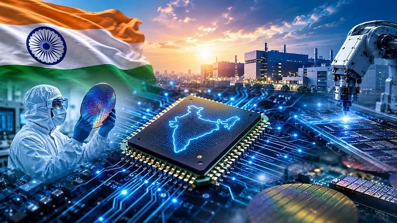
India notified the Rs 1.27 lakh crore Semicon 2.0 scheme, recalibrating capital subsidies for silicon fabs to 40% while extending financial backing to equipment, raw materials, specialty gases, and localized chip design IP to build a self-reliant domestic semiconductor supply chain.
NEW DELHI — The Indian government officially notified the Rs 1,27,500-crore Semicon 2.0 framework on Monday, shifting its strategic focus from capital-heavy fabrication plants toward building a comprehensive, self-reliant domestic chip ecosystem. Spearheaded by the Ministry of Electronics and Information Technology (MeitY) and executed through the India Semiconductor Mission (ISM), the updated policy recalibrates capital subsidies for silicon fabrication units while expanding fiscal incentives to cover equipment manufacturing, specialty chemicals, industrial gases, raw materials, intellectual property design, and workforce training. This rollout marks a critical turning point for South Asia’s technology sector as policymakers attempt to transition the country from a pure assembly hub into an integrated global semiconductor powerhouse.
Broadening the Framework Across Six Pillars
Under the newly released guidelines, Semicon 2.0 distributes capital support across six distinct operational pillars: chip design, semiconductor equipment and materials, silicon and compound fabs, assembly, testing, marking, and packaging (ATMP/OSAT), research and development, and talent development.
While the initial phase—Semicon 1.0, launched in December 2021 with a Rs 76,000-crore outlay—concentrated primarily on drawing large-scale fabrication and basic packaging plants with flat 50 percent subsidies, the new phase recalibrates these incentives. Silicon semiconductor fabrication facilities will now receive a 40 percent capital expenditure subsidy, while compound-semiconductor fabs, display units, and specialized facilities are eligible for 35 percent. Concurrently, the state is extending a 30 percent capital expenditure incentive to manufacturers of critical equipment, raw materials, and specialized gases, alongside a production-linked incentive of up to 10 percent on domestic bill-of-material values.
Strategic Design Ownership and Domestic IP
A central structural change in Semicon 2.0 involves strict localization conditions governing the chip design pillar. Intellectual property developed under the strategic category must be co-owned by the applicant and the state-backed Centre for Development of Advanced Computing (C-DAC), with all foundational design files mandated to remain within India.
Eligibility for this strategic design category is restricted to entities incorporated, headquartered, and controlled by Indian citizens, though companies owned by Overseas Citizens of India (OCIs) are cleared to participate on the commercial side. An expert panel jointly chaired by the Principal Scientific Adviser and the National Security Adviser will evaluate and classify strategic chips across six core groups: compute, memory, radio frequency, power, networking, and sensors.
Impact on Industry, Investors, and Technology Supply Chains
The policy evolution carries immediate consequences for international investors, domestic electronics manufacturers, and global supply chain strategists. By incentivizing local production of high-purity chemicals, gases, and precision machinery, the government aims to insulate local electronics output from international supply shocks and reduce systemic vulnerabilities.
For commercial enterprises and startups, the framework lowers entry barriers by offering seed funding of up to Rs 15 crore—or half the project cost—alongside equity co-investment mechanisms. Market analysts note that these provisions are designed to foster indigenous microchip architectures, lessen reliance on imported components for critical infrastructure, and stimulate long-term precision manufacturing.
Official Sources Section
The details of this initiative are drawn from official policy notifications and public briefings issued by the Ministry of Electronics and Information Technology (MeitY), administrative directives published by the India Semiconductor Mission (ISM), and official statements delivered by Union Cabinet officials.
Quote Section
According to officials, global semiconductor stakeholders have demonstrated increasing confidence in India's long-term manufacturing roadmap, establishing the nation as a reliable destination for capital deployment over the coming decades. Organizers stated that the updated framework will act as a catalyst for more than Rs 5 lakh crore in cumulative private and industry investments over the next five to seven years.
Why It Matters
The structural pivot from Semicon 1.0 to Semicon 2.0 addresses a fundamental vulnerability of modern electronics production: owning a fabrication plant does not secure a supply chain if raw silicon wafers, electronic design automation (EDA) tools, electronic gases, and packaging sub-components must be entirely imported. By underwriting domestic equipment manufacturing and safeguarding sovereign chip designs, the policy attempts to build durable technical depth rather than temporary assembly capacity. This reduces exposure to geopolitical choke points and positions domestic firms to capture higher margins in global technology trade.
Key Facts at a Glance
Total Financial Outlay: Rs 1,27,500 crore allocated across the updated multi-pillar policy framework.
Adjusted Fab Subsidies: Silicon fabrication plants receive 40 percent capital support, down from the flat 50 percent under phase one, while compound and display fabs receive 35 percent.
New Supply Chain Focus: Introduces targeted fiscal support for machinery, industrial gases, specialty chemicals, and raw material providers.
Design Localization: Strategic chip designs must be co-owned by C-DAC and retained within India under strict national security guidelines.
FAQ Section
What is the primary difference between Semicon 1.0 and Semicon 2.0?
While the first phase concentrated heavily on subsidizing large-scale silicon fabrication and assembly plants, Semicon 2.0 broadens its financial support to encompass the entire upstream ecosystem, including raw materials, specialty gases, precision machinery manufacturing, and sovereign chip design IP.
How much capital support do new fabrication plants receive under the updated scheme?
Silicon semiconductor fabrication units are eligible for a 40 percent capital expenditure subsidy, while compound-semiconductor and display fabs qualify for 35 percent support.
Who is eligible to apply for the strategic chip design incentives?
Applications under the strategic design category are restricted to entities incorporated, headquartered, and controlled by Indian citizens, with participation rights also extended to companies owned by Overseas Citizens of India (OCIs) on the commercial side.
What role does the India Semiconductor Mission play in the rollout?
The India Semiconductor Mission (ISM) acts as the central nodal agency responsible for reviewing project applications, coordinating implementation across all six pillars, and overseeing the execution of the framework.
Source: Ministry of Electronics and Information Technology (MeitY), India Semiconductor Mission (ISM), Union Cabinet Policy Releases.