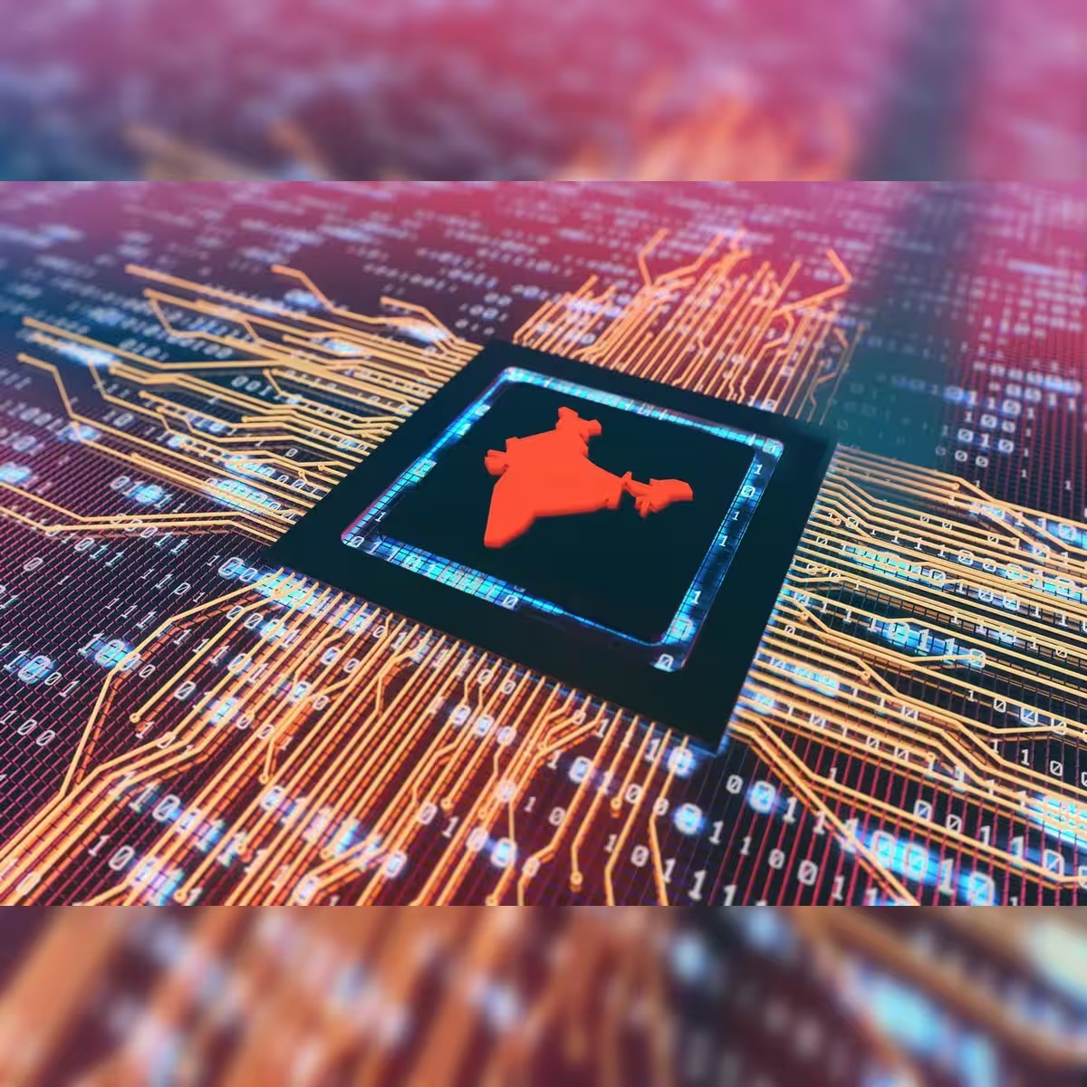
India has launched the ₹1.275 lakh crore India Semiconductor Mission 2.0, placing domestic chip design startups at the center of its tech strategy. Through equity co-investment alongside private venture capital, the program aims to build indigenous intellectual property, fund expensive tape-outs, and prevent early foreign buyouts of local semiconductor innovators.
NEW DELHI — The Union Cabinet's approval of the second phase of the India Semiconductor Mission (ISM 2.0) with a fiscal outlay of ₹1.275 lakh crore (over ₹1.25 lakh crore) marks a fundamental strategic shift in India's technology policy toward domestic microchip design and intellectual property ownership. Approved by the central government following clearances from the Ministry of Electronics and Information Technology (MeitY) and the Finance Ministry's Expenditure Finance Committee, the six-year initiative expands upon the initial ₹76,000 crore rollout launched in 2021. By co-investing alongside private venture capital funds into high-potential chip design startups, India is shifting focus from raw manufacturing assembly toward high-value semiconductor IP creation.
Strategic Pivot: Prioritizing High-Value Chip Design Startups
While the first phase of the India Semiconductor Mission centered on attracting mega-scale silicon fabrication plants and assembly, testing, marking, and packaging (ATMP/OSAT) facilities, India Semiconductor Mission 2.0 pivots strongly toward the fabless design segment. Global semiconductor industry data shows that chip design accounts for nearly 50 percent of total value addition across the global semiconductor value chain.
Though India hosts over 20 percent of the world’s semiconductor design engineering workforce, the vast majority of intellectual property historically created within the country has been held by multinational technology firms. Under India Semiconductor Mission 2.0, the government seeks to foster native chip startups that own full-stack Indian IP, assisting emerging companies through the capital-intensive process of tape-outs—the final phase of microchip design before commercial manufacturing.
Through the revised Design Linked Incentive (DLI) framework, MeitY has already supported over 100 startups with access to advanced Electronic Design Automation (EDA) tools and foundry tape-out grants. The second phase dramatically scales this financial support to help Indian design firms develop advanced chips tailored for artificial intelligence (AI), 5G/6G telecommunications, automotive electronics, and defense systems.
Co-Investment Model to Anchor Indigenous Intellectual Property
A cornerstone innovation of India Semiconductor Mission 2.0 is the introduction of a government co-investment scheme. Designing advanced microchips at cutting-edge nodes requires capital expenditures ranging from ₹500 crore to over ₹1,000 crore per architecture—outpacing the reach of traditional grant-based incentives.
Under the new equity matching model, the central government will match private investments made by whitelisted venture capital and private equity firms into Indian chip startups. This dual structure provides two distinct advantages:
Market-Driven Validation: Venture capital involvement ensures that state funds flow to commercially viable chip architectures with clear market demand.
Protection Against Early Buyouts: Long-term patient capital backed by the state prevents promising Indian design startups from being acquired prematurely by foreign technology conglomerates before reaching global scale.
In addition to equity co-investments, the government will offer deployment-linked incentives and royalty-based payout models to encourage local systems manufacturers to integrate home-grown chips into commercial products.
Scaling Beyond Fabrication to Supply Chain and Equipment
Beyond chip design, India Semiconductor Mission 2.0 expands state subsidies across six strategic pillars:
Semiconductor Equipment & Specialty Materials: Incentivizing local manufacturing of ultra-pure gases, specialized chemicals, and high-precision machinery.
Advanced Packaging & Fabs: Providing 40% capital expenditure support for silicon fabs and 35% for compound semiconductors and OSAT facilities.
Talent & University Ecosystems: Expanding hands-on EDA chip design and fabrication training across more than 300 Indian universities.
By addressing the full semiconductor supply chain—from initial architectural design to chemical supply and final packaging—the government aims to locally design and manufacture chips for up to 75 percent of domestic electronic applications over the coming years.
Official Sources Section
All policy frameworks, fiscal outlays, and program objectives detailing India Semiconductor Mission 2.0 are documented in public statements and regulatory updates issued by the Ministry of Electronics and Information Technology and the official portal of the India Semiconductor Mission. Financial allocations are aligned with budget approvals monitored by the Ministry of Finance.
Quote Section
According to official statements from Ministry of Electronics and IT Secretary S. Krishnan regarding the design incentives under the new phase:
"To design high-end chips you need ₹1,000 crore or more. At the same time, the government can't give everything. This is why you have this combination saying that when whitelisted venture capitalist funds invest, we will co-invest. The idea is to increase overall funding and ensure Indian companies retain domestic IP rather than being sold early."
Why It Matters
By channeling substantial funding into indigenous design startups under India Semiconductor Mission 2.0, India seeks to move up the technology value chain from an assembly hub to a owner of core semiconductor intellectual property. For local hardware businesses, electronics manufacturers, and defense contractors, a domestic chip design ecosystem reduces long-term reliance on foreign supply chains while enhancing national security and economic resilience against global silicon shortages.
Key Facts at a Glance
Expanded Outlay: ₹1.275 lakh crore (over ₹1.25 lakh crore) allocated for India Semiconductor Mission 2.0 over a six-year period.
Equity Co-Investment: Government will match venture capital funding into domestic chip design startups to build high-end IP.
Design Incentive Expansion: Covers expensive foundry tape-outs, advanced EDA tool licenses, and deployment incentives.
Supply Chain Focus: Extends subsidies to equipment manufacturing, specialty chemicals, compound fabs, and talent training across 300+ universities.
FAQ Section
What is India Semiconductor Mission 2.0 (ISM 2.0)?
India Semiconductor Mission 2.0 is the second phase of India's national semiconductor program, backed by a ₹1.275 lakh crore budget to strengthen domestic chip design, equipment manufacturing, specialty materials, and chip packaging.
Why is the government focusing heavily on chip design startups?
Chip design represents up to 50 percent of the value addition in semiconductors. By supporting domestic fabless startups, India aims to own core intellectual property rather than relying solely on foreign-designed chips.
How does the government's equity co-investment model work?
To help startups fund capital-intensive chip development (which can cost ₹1,000 crore or more), the government co-invests alongside approved venture capital funds, providing patient capital while ensuring market validation.
How can official policy updates on ISM 2.0 be tracked?
Official notices and guidelines are published directly on the portal of the India Semiconductor Mission and MeitY.
Source: India Semiconductor Mission, Ministry of Electronics and Information Technology, Ministry of Finance