India's newly approved ₹1.27 lakh crore Semicon 2.0 programme introduces a co-investment equity framework to fund advance chips design by Indian companies. By matching venture capital investments, the government aims to overcome the high capital costs of engineering sub-7nm AI chips, securing long-term technological self-reliance.
NEW DELHI — The Union Cabinet's approval of the ₹1.27 lakh crore ($14 billion) Semicon 2.0 programme marks a major strategic shift in India’s semiconductor policy, transitioning the domestic ecosystem from basic electronics assembly toward self-reliance in advanced technology development. Designed to run for six years starting in the fiscal year 2027 (FY27), the newly modified initiative introduces strict equity-matching and co-investment models.
This framework is specifically targeted at attracting the massive private capital required for advance chips design by Indian companies, directly positioning the nation as a global hub for semiconductor intellectual property (IP).
Overcoming the Capital Bottleneck for High-End Silicon
The domestic semiconductor design sector has historically faced severe growth-capital hurdles. Under previous policy frameworks, such as the initial Design-Linked Incentive (DLI) scheme, financial support was capped at roughly ₹15 crore per project. While sufficient for entry-level applications, this baseline funding fell drastically short of the immense capital required to engineer next-generation microprocessors.
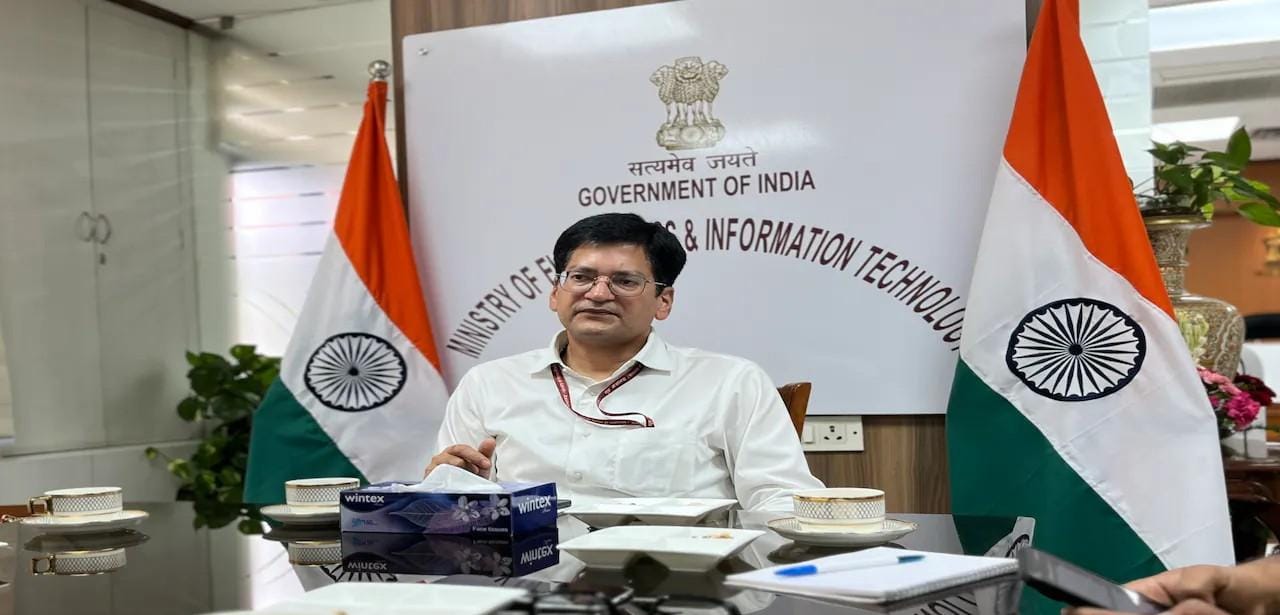
In an interview, Ministry of Electronics and IT Secretary S. Krishnan emphasized that designing high-end, advance chips requires investments scaling past ₹1,000 crore. Because public funding cannot entirely cover these vast engineering costs, Semicon 2.0 establishes a co-investment mechanism.
Under these new equity norms, the central government will directly match the funding brought in by whitelisted venture capital (VC) firms. This strategy shifts the responsibility of technical vetting and commercial selection onto professional investors, while simultaneously leveraging public funds to expand the total pool of risk capital available to domestic tech startups.
Shifting from Basic Utility to Sovereign IP Creation
The primary objective of Semicon 2.0 is to build deep domestic competencies in designing sub-7 nanometer (nm) nodes, which are essential for powering sophisticated artificial intelligence systems, satellite communications, and advanced defense infrastructure. Currently, India's upcoming commercial fabrication units—such as the country's first commercial silicon fab scheduled to be commissioned in 2028—will focus on legacy 28nm nodes typically used in power electronics and automotive systems.
While the commercial manufacturing of sub-7nm advance chips inside India will take significantly longer to manifest, the government’s immediate priority is ensuring that the foundational intellectual property and systems architectures are engineered domestically over the next six years.
Official Sources Section
According to official updates from the Press Information Bureau (PIB) and regulatory documentation from the India Semiconductor Mission (ISM), the central government has already whitelisted 105 startups and MSMEs that are actively developing domestic chips. Under the direction of the Union Cabinet chaired by Prime Minister Narendra Modi, the six-pillar scheme will provide financial support in the form of direct grants, equity stakes, or royalty-linked repayments to eliminate the high upfront tape-out costs that restrict early-stage hardware engineering.
Executive Commentary
"We intend to provide more funding. Otherwise, under the design-linked incentive scheme, you get only about ₹15 crore. Now, to design high-end chips you need ₹1,000 crore or more," stated Ministry of Electronics and IT Secretary S. Krishnan during a media brief.
"At the same time, the government can't give everything. This is why you have this combination saying that you get investment from a venture capitalist or somebody who believes that you will be able to bring out this chip, and we will co-invest."
Addressing the operational limitations of state agencies, Krishnan added: "The idea of co-investment is two-fold. One, that we increase the overall funding, which is available. Two, the government doesn't do the selection because it doesn't have that capacity. When whitelisted venture capitalist funds invest, we will co-invest."
Why It Matters
For venture capitalists and institutional investors, the introduction of equity-matching provides a state-backed de-risking mechanism, effectively cutting the capital exposure required to fund hardware engineering in half. For domestic technology startups, this model allows access to world-class electronic design automation (EDA) tools and complex tape-outs without surrendering operational control to bureaucratic bodies, as the government maintains a passive financial stake capped below 50%.
On a broader macroeconomic scale, establishing sovereign ownership over chip designs protects national critical infrastructure—including telecommunications, smart grids, and aerospace—from foreign supply chain blockades and malicious hardware vulnerabilities.
Key Facts at a Glance
Total Program Outlay: Backed by an expanded, dedicated central budget of ₹1,27,500 crore ($14 billion) approved by the Union Cabinet.
Operational Timeline: The comprehensive Semicon 2.0 framework will remain active for six years, officially taking effect starting in FY27.
Funding Architecture: Implements a co-investment equity model for startups alongside a 1.5x royalty-based repayment structure for large corporate entities.
Targeted Startups: The India Semiconductor Mission has already identified and mapped 105 startups engaged in domestic chip design.
Core Technological Node Focus: Aims to catalyze advance chips design categorized by highly complex sub-7 nanometer nodes.
Frequently Asked Questions
What defines an "advance chip" under the new Semicon 2.0 guidelines?
Advance chips are formally classified as semiconductors that utilize highly complex sub-7 nanometer (nm) nodes and smaller processing architectures, heavily required for modern artificial intelligence systems.
Will the Indian government take operational control of startups via these equity norms?
No. The India Semiconductor Mission (ISM) has clarified that the government will act purely as a financial investor, keeping its equity stake below 50% without seeking operational control or board management seats.
Can startup founders buy back the equity from the government later on?
Yes. Once an Indian chip design company matures and begins generating commercial revenue, the founders are given clear structural paths to buy back the state's equity stake at prevailing market valuations.
Source: Official press statements and data releases retrieved from the Ministry of Electronics and Information Technology, the India Semiconductor Mission, and the Press Information Bureau.