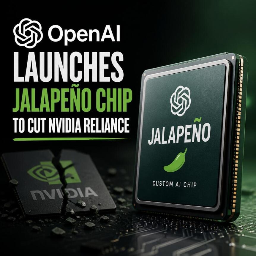
OpenAI has unveiled its first custom AI processor, "Jalapeño," developed in a nine-month cycle with Broadcom. Built as a specialized inference ASIC rather than a general GPU, the chip aims to improve performance-per-watt metrics, lower ChatGPT operational costs, and reduce long-term reliance on external chip suppliers.
SAN FRANCISCO — In a direct bid to establish operational autonomy over its infrastructure, OpenAI has officially unveiled its first custom-designed silicon chip, named "Jalapeño." The corporate development, introduced on Wednesday, June 24, 2026, marks the tech company's transition from a pure software developer into an integrated full-stack hardware platform.
Co-developed alongside semiconductor manufacturer Broadcom, the custom silicon is explicitly architected as an application-specific integrated circuit (ASIC) rather than a general-purpose graphics processing unit (GPU). The deployment targets "inference" the computing framework that powers real-time user calculations whenever artificial intelligence interfaces like ChatGPT, Codex, or underlying enterprise APIs generate automated responses. By engineering its own silicon parameters, OpenAI aims to lower computing overhead costs, bypass global hardware supply shortages, and expand access to its consumer and enterprise products.
A "Blank-Slate" ASIC Built to Solve AI's Costly Power Problem
Unlike conventional hardware setups, which typically modify legacy graphic processing engines to handle machine learning tasks, Jalapeño was developed from a "blank-slate" layout. OpenAI optimized the internal compute matrix around specialized model execution patterns, custom software kernels, and data-movement paths. By matching memory architecture directly with large language model (LLM) requirements, the system significantly reduces data transit bottlenecks, allowing the processor to execute workloads much closer to its theoretical maximum peak efficiency.
The strategic priority of the hardware program leans heavily on optimizing energy use rather than raw computing speed. Data centers globally face strict limitations regarding the electricity they can reliably draw from the power grid. In early laboratory validations, engineering samples running active models including the unreleased GPT-5.3-Codex-Spark network demonstrated performance-per-watt efficiency that is substantially better than today's leading-edge accelerators.
This reduction in power consumption enables hosting centers to run massive, multi-turn conversational agents with a lower aggregate energy footprint.
Nine-Month Development Cycle Accelerated by In-House AI Models
The manufacturing timeline of the chip represents a highly accelerated design-to-tape-out window for advanced semiconductors. The custom chip program moved from its early concept phase to finalized manufacturing tape-out in just nine months. According to engineering project summaries, this speed was made possible by deeply integrating OpenAI’s own generative software models into the physical silicon engineering process.
Engineers deployed advanced LLM layouts to automate parts of the chip design, trace complex circuit routing, and verify hardware placement optimization. This unique feedback loop allowed the AI systems served to everyday consumers to help refine and build the underlying physical hardware layers required to run future models.
The industrial packaging and commercialization of the project rely on a broad network of technology partners. While OpenAI researchers controlled the fundamental architecture, Broadcom handled the physical silicon design and high-performance Tomahawk networking integration. The actual physical manufacturing is managed by Taiwan Semiconductor Manufacturing Company (TSMC), while Celestica serves as the infrastructure partner responsible for assembling the custom boards, server racks, and data center housing systems.
Following the Path of Silicon Independence Across Tech Giants
The rollout of Jalapeño positions OpenAI alongside global technology conglomerates that have developed independent silicon divisions to bypass external market monopolies. For years, the advanced AI ecosystem has relied on Nvidia's specialized hardware, creating high acquisition costs and extensive supply lead times.
By developing custom ASICs, OpenAI mirrors long-term infrastructure choices implemented by peers like Alphabet (Google), which utilizes its custom Tensor Processing Units (TPUs) to run the Gemini engine, and Microsoft, which recently deployed its Maia 200 inference accelerator. Initial deployments of Jalapeño are scheduled to launch in late 2026 within gigawatt-scale data center ecosystems operated alongside Microsoft and secondary cloud partners.
Official Sources Section
The hardware structures, collaborative project agreements, and operational timelines featured in this report match the technical data released directly by the engineering groups:
Quote Section
"Jalapeño is part of our long-term full-stack infrastructure strategy to make compute more abundant, resulting in AI which is faster, more reliable, and more affordable for people and businesses," stated OpenAI President Greg Brockman in a joint corporate announcement. "By designing more of the stack ourselves, we can serve more intelligence with greater efficiency and keep pushing advanced AI toward broader access".
Why It Matters
The shift to bespoke inference silicon alters the economic landscape of consumer artificial intelligence. For businesses and independent developers building products on top of public APIs, hardware operations using general-purpose GPUs create variable, high processing costs that complicate long-term budgeting. Custom ASICs designed specifically for LLM workflows cut real-world operational costs by up to 50 percent compared to legacy hardware. This cost reduction allows software providers to offer faster response times, scale up complex coding tools, and lower end-user subscription fees while maintaining steady profit margins.
Key Facts at a Glance
Custom ASIC Debut: OpenAI has introduced Jalapeño, its first custom-designed processor built specifically for large language model inference.
Nine-Month Turnaround: The semiconductor design process reached a complete manufacturing tape-out in nine months, accelerated by OpenAI’s own AI models.
Power Optimization: Early testing indicates that the chip offers substantial performance-per-watt improvements over conventional state-of-the-art accelerators.
Ecosystem Alliances: Developed alongside Broadcom, the hardware will be manufactured by TSMC and deployed within Microsoft data networks starting in late 2026.
Industry Compatibility: The silicon architecture is designed with the flexibility to execute and optimize both proprietary and third-party open-source LLM frameworks.
FAQ Section
Q1: Is OpenAI’s Jalapeño chip designed to compete with Nvidia for training large models?
No. Jalapeño is an application-specific integrated circuit (ASIC) built exclusively for inference the process of running pre-existing models to answer user queries rather than the intensive initial training phase.
Q2: How did artificial intelligence models assist in building the new processor?
OpenAI utilized its own large language models to accelerate parts of the semiconductor development process, automating structural circuit layout verification and optimizing internal memory-movement networks.
Q3: When will regular users experience the impact of the new silicon?
Initial data center deployments are slated to begin by the end of 2026. As the hardware scales, users can expect faster response times and fewer system outages during peak usage periods.
Q4: Will this chip design be used exclusively for ChatGPT?
No. OpenAI and Broadcom confirmed that Jalapeño possesses the structural flexibility to support current and future LLM architectures deployed across the broader technology industry.
Source: Official Joint Infrastructure Press Announcements published by OpenAI and Broadcom Investor Relations, alongside verified semiconductor manufacturing registries.