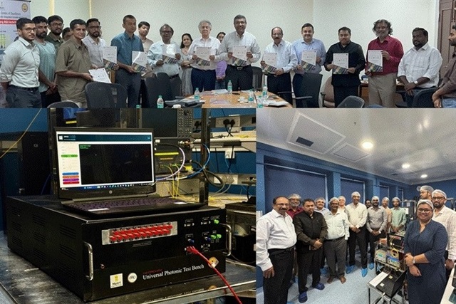
India’s Ministry of Electronics and Information Technology (MeitY) has launched two indigenously developed silicon photonics tools at IIT Madras. Featuring a Process Design Kit (PDK) with over 50 verified components and an automated testing engine, the national platform democratizes access to advanced photonic chip design for researchers, defense labs, and technology startups.
CHENNAI — The Ministry of Electronics and Information Technology (MeitY) has officially launched India's first indigenously developed silicon photonics design and testing ecosystem at the Indian Institute of Technology Madras (IIT Madras). Unveiled by MeitY Secretary S. Krishnan alongside India Semiconductor Mission (ISM) CEO Amitesh Sinha, the new tools include a Silicon Photonics Process Design Kit (PDK) and a Universal Programmable Photonic Integrated Circuit (PPIC) Test Engine. Developed at the MeitY-sponsored Centre of Excellence for Compound Photonics and Photonic Integrated Circuits Systems (CoE-CPPICS), this initiative establishes a shared national infrastructure intended to accelerate semiconductor research, commercial startup development, and defense innovation across the country.
Breakthrough in Indigenous Semiconductor Design
Silicon photonics replaces traditional copper interconnects with microscopic optical signals, enabling microchips to transfer data using light rather than electrical currents. This transition offers up to 100 times faster data transmission rates while significantly reducing power consumption—a critical requirement for next-generation artificial intelligence data centers, telecommunications networks, and quantum processing units.
Prior to this development, Indian academic institutions, defense laboratories, and chip startups relied on imported software libraries and foreign test beds, which often incurred high license fees and export restrictions. By introducing homegrown silicon photonics tools, India aims to establish technological sovereignty in photonic integrated circuit (PIC) design and lower the barrier to entry for domestic hardware innovators.
Technical Architecture of the PDK and Test Platform
The newly released Silicon Photonics Process Design Kit provides a comprehensive digital component library comprising over 50 independently verified optical building blocks. These components allow engineers to model, simulate, and lay out complex photonic circuits—such as waveguides, optical modulators, splitters, and photodetectors—compatible with standard complementary metal-oxide-semiconductor (CMOS) manufacturing lines.
To complement the design kit, CoE-CPPICS developed the Universal PPIC Test Engine. This automated characterization platform enables automated testing and validation of packaged photonic modules without requiring researchers to ship physical prototypes to overseas laboratories. Operating on a Product Research, Development, and Manufacturing (PRDM) model, the center leverages foundry partnerships, including SilTerra Malaysia for wafer fabrication and Bengaluru-based izmo Microsystems for advanced photonic packaging.
Expanding Access for Academia, Industry, and Defense
Operating as an open-access national facility, the silicon photonics toolkit is structured to support multi-project wafer (MPW) fabrication runs, enabling multiple research groups and private startups to share manufacturing costs on a single silicon wafer.
For domestic technology startups, the availability of verified design tools reduces upfront research and development capital requirements. Academic institutions gain hands-on access to production-ready chip blueprints, while defense research organizations can design secure optical communication components and quantum sensors locally without risking sensitive intellectual property.
Strategic Roadmap Under the India Semiconductor Mission
During the official launch ceremony, government officials outlined plans to integrate silicon photonics research directly into future funding phases under the India Semiconductor Mission. As artificial intelligence workloads drive global demand for optical interconnects, India's strategy focuses on building local fabrication and packaging infrastructure to match international technical standards.
MeitY officials indicated that commercialization results from the current multi-project wafer runs will inform proposals for setting up dedicated domestic commercial silicon photonics fabrication facilities under the upcoming ISM 2.0 framework.
Official Sources Section
Information in this news report is based on official announcements published by the Press Information Bureau, institutional press briefings from the Ministry of Electronics and Information Technology, research documentation from IIT Madras, and strategic program guidelines issued by the India Semiconductor Mission.
Quote Section
"According to officials from the Ministry of Electronics and Information Technology, India's progress in silicon photonics is approaching global benchmarks, creating a foundation that will be supported by upcoming research initiatives under the India Semiconductor Mission."
Why It Matters
For domestic researchers, hardware startups, and engineering students, access to homegrown silicon photonics tools eliminates dependence on costly foreign software licenses and restrictive overseas test facilities. For telecom providers, data centers, and defense agencies, locally designed optical chips offer faster processing speeds, lower energy consumption, and stronger supply chain security for critical communications infrastructure.
Key Facts at a Glance
Core Launch: India’s first indigenously developed Silicon Photonics Process Design Kit (PDK) and Universal PPIC Test Engine.
Lead Institutions: Developed by CoE-CPPICS at IIT Madras with backing from MeitY.
Design Capability: The PDK includes over 50 verified optical components for custom chip design.
Access Model: Functions as a shared national facility for universities, startups, industry partners, and defense labs.
Future Objective: Lays the technical groundwork for establishing dedicated silicon photonics fabrication facilities under ISM 2.0.
FAQ Section
What are silicon photonics tools, and why are they important?
Silicon photonics tools allow engineers to design microchips that transmit data using light particles (photons) instead of electrical currents, enabling faster data transfer speeds and lower energy consumption in computing systems.
Who can access these homegrown silicon photonics tools in India?
The tools are available through a shared national facility at IIT Madras to academic researchers, private startups, industrial manufacturers, and defense R&D organizations.
What is included in the new Silicon Photonics PDK?
The Process Design Kit contains a verified digital library of over 50 photonic components, allowing chip designers to build and simulate optical integrated circuits locally.
How does this project support the India Semiconductor Mission?
By establishing domestic chip design capabilities and testing infrastructure, the project creates the technological foundation required to support commercial silicon photonics manufacturing facilities under future semiconductor policy phases.
Source: Press Information Bureau, Ministry of Electronics and Information Technology, IIT Madras, India Semiconductor Mission