India is seeking semiconductor manufacturing investments and multilateral funding at the Pax Silica Summit in Washington, D.C. Senior technology officials are leveraging the 16-nation, U.S.-led alliance to showcase India's expanding chip assembly and design ecosystems, while unlocking access to a $250 million seed fund and global sovereign capital networks.
Senior technology officials leverage the 16-nation multilateral summit to attract semiconductor manufacturing capital and unlock specialized funding networks.
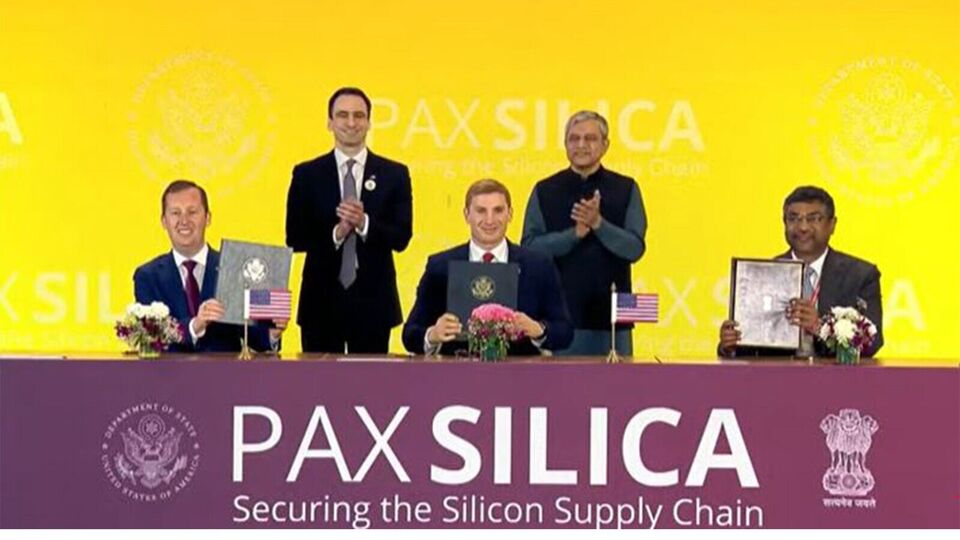
WASHINGTON — Senior diplomatic and technology delegations from India have arrived in Washington, D.C., to actively participate in the second summit of the U.S.-led 16-nation Pax Silica coalition. Running from June 25 to June 26, 2026, the diplomatic assembly serves as a critical stage for New Delhi to secure multi-billion-dollar semiconductor chip investments and integrate into western artificial intelligence (AI) infrastructure playbooks.
The strategy is vital today as leading economies try to restructure critical supply chains, establish resilient technology networks, and safeguard the global "silicon stack" from overconcentration and external economic coercion.
Accelerating India’s Semiconductor Ecosystem on the Global Stage
According to official briefings from the Ministry of Electronics and Information Technology (MeitY) and the Ministry of External Affairs (MEA), India's delegation is using the two-day Washington summit to showcase its rapidly maturing domestic microelectronics sector. The targeted push builds upon India's formal integration into the Pax Silica alliance during the India AI Impact Summit held earlier this year.
At the core of India’s presentation is its expanding semiconductor infrastructure ecosystem. Senior officials are highlighting recent breakthroughs across the full production lifecycle, including advanced wafer fabrication pipelines, domestic integrated circuit design houses, and high-capacity Assembly, Testing, Marking, and Packaging (ATMP) projects. By outlining these developments alongside a vast consumer internal market, New Delhi aims to pitch itself as a safe, highly stable alternative destination for global technology manufacturing.
Accessing the Pax Silica Seed Fund and Global Capital Pipelines
A primary goal for the Indian delegation during the bilateral and multilateral discussions is gaining strategic access to the United States-backed Pax Silica seed fund. This specialized $250 million financing mechanism was created as a foreign assistance and developmental support tool, specifically tailored to finance critical mineral extraction, raw material processing facilities, and strategic hardware assets across signatory territories.
While administrative officials acknowledge that a $250 million baseline fund is not large enough on its own to bankroll capital-intensive semiconductor fabrication plants, its true value lies in institutional de-risking. The United States Department of State indicated that the alliance is designed to catalyze and direct capital from massive global sovereign wealth funds and private equity firms managing more than $1 trillion in combined assets.
Furthermore, Indian tech representatives are leveraging the summit to advance discussions on co-investment opportunities involving American semiconductor firms. These talks follow groundwork established during earlier bilateral visits, including Foreign Secretary Vikram Misri's trip to the U.S. and Secretary of State Marco Rubio’s high-level trade mission to India.
Expanding the Geopolitical Tech Coalition
The current Washington summit marks an expansion of the Pax Silica framework, which was originally established by the U.S. State Department to secure AI supply chains encompassing minerals, data centers, and advanced processors. The alliance has recently grown to include the European Union, Germany, and the Netherlands—jurisdictions that hold highly concentrated, irreplaceable semiconductor lithography capabilities and manufacturing machinery.
The inclusion of these European tech powers gives India a direct channel to forge wider industrial partnerships. By building reliable ties with trusted partners that share its open economic values, India is actively positioning its skilled engineering workforce to fill global talent gaps, with the local chip sector projected to require nearly one million trained professionals over the next decade.
Official Sources Section
The diplomatic priorities, delegation objectives, and project funding pipelines detailed in this report are verified by statutory press releases published by the Press Information Bureau (PIB) on behalf of the Ministry of Electronics and Information Technology (MeitY), India. Operational framework parameters and alliance goals are mapped in accordance with official programmatic fact sheets compiled by the [suspicious link removed].
Quote Section
"According to officials and diplomatic statements issued during the initial bilateral sessions, the Pax Silica coalition serves as a purpose-built platform to manage the evolving AI economy. The goal is to build deep, resilient collaboration with trusted international partners who share common democratic values, ensuring long-term supply chain security."
Why It Matters
Securing deep institutional ties through the Pax Silica summit gives India the necessary leverage to insulate its domestic industries from geopolitical supply drops. For electronic manufacturers, automotive corporations, and consumer technology firms inside India, localized chip production translates to lower import costs and protection from international component shortages. For global investors, the backing of a U.S.-led multilateral pact provides the legal and financial predictability required to commit long-term capital to India’s industrial zones.
Key Facts at a Glance
Summit Venue: The second Pax Silica Summit is being hosted by the U.S. State Department in Washington, D.C.
Core Agenda: Focuses on securing advanced AI infrastructure, critical mineral corridors, and semiconductor manufacturing.
Funding Catalyst: India is targeting access to the $250 million Pax Silica seed fund to mobilize private investments from a $1 trillion capital pool.
New Coalition Members: The European Union, Germany, and the Netherlands have officially joined the strategic technology pact.
Domestic Focus: India is presenting its ATMP packaging footprint and engineering talent to capture next-generation data center investments.
FAQ Section
Q1: What is the Pax Silica Summit being held in Washington? A1: It is a high-level strategic conference led by the U.S. State Department focused on building secure, resilient supply chains for semiconductors, critical minerals, and artificial intelligence infrastructure among trusted allied nations.
Q2: What is India's primary goal at the Pax Silica Summit? A2: India aims to attract global semiconductor manufacturing investments, expand trade linkages for its chip design and assembly sectors, and secure funding from the alliance's specialized financial networks.
Q3: What is the Pax Silica seed fund? A3: The seed fund is a $250 million foreign assistance and financing mechanism backed by the U.S. to support infrastructure, critical mineral processing, and tech manufacturing assets across member states.
Q4: Which new members have recently joined the Pax Silica alliance? A4: The European Union, the Netherlands, and Germany have officially joined the coalition, significantly boosting the alliance's semiconductor equipment and fabrication capabilities.
Source: Press Information Bureau (PIB) India