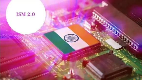

The Indian government has approved the ₹1.27 lakh crore Semicon 2.0 mission, a transformational initiative aimed at building a robust domestic semiconductor ecosystem. By focusing on design, manufacturing, materials, and talent, the mission seeks to position India as a global hub for electronics and chip production by 2035.
NEW DELHI — The Union Cabinet, led by Prime Minister Narendra Modi, has officially approved the second phase of the India Semiconductor Mission (ISM), known as Semicon 2.0. With a massive fiscal outlay of ₹1,27,500 crore, this initiative aims to transform India from a chip design hub into a comprehensive global powerhouse for semiconductor manufacturing, packaging, and research.
This development comes as India looks to build on the momentum of Semicon 1.0, which successfully established credibility in the sector with several fabrication and packaging plants already becoming operational. The second phase is designed to create a resilient and self-reliant semiconductor ecosystem, essential for modern digital and industrial infrastructure.
A Transformational Step for Global Competitiveness
Ashok Chandak, CEO and President of SEMI India and the India Electronics and Semiconductor Association (IESA), described ISM 2.0 as a "transformational step." According to Chandak, the policy provides the necessary continuity and government commitment required to attract global players, who are vital for bringing advanced process know-how and technology to India.
The new phase shifts the focus from mere chip design to a holistic ecosystem approach. While the first phase established India's footprint in design, Semicon 2.0 targets deep integration into the global supply chain by incentivizing the production of semiconductor equipment, essential chemicals, and industrial gases.
Six Pillars of the Semicon 2.0 Strategy
The government has structured Semicon 2.0 around six strategic pillars to ensure long-term sustainability and technological sovereignty:
Chip Design: Building on the success of 105 startups already working on chip designs, the government plans to deepen the ecosystem by developing strategic intellectual property (IP) and system-level blocks.
Machines and Materials: Incentivizing local R&D and manufacturing for equipment, chemicals, and gases to support fab operations.
Fabs and Manufacturing: Supporting silicon, compound semiconductor, and display fabs to meet demand across automotive, telecom, and aerospace sectors.
Advanced Packaging (ATMP/OSAT): Encouraging the adoption of the latest packaging technologies to position India as an alternative global hub for chip assembly.
Research & Development: Collaborating with global R&D centers to move beyond the current 28nm–110nm nodes toward more advanced technology nodes.
Talent Development: Expanding training programs that have already upskilled 68,000 students to ensure a steady pipeline of workforce-ready engineers.
Why It Matters
For businesses and investors, the long-term policy support and substantial budget outlay provide the stability needed for the multi-billion dollar investments required for fabrication units. By strengthening the supply chain and fostering domestic IP, India aims to reduce its strategic vulnerability to global chip shortages and align itself with a more resilient global semiconductor network. For the average citizen, the mission promises to bolster national security, foster high-value employment, and support the growth of sectors like 5G, electric mobility, and AI.
Key Facts at a Glance
Total Outlay: ₹1,27,500 crore approved for the next phase of the programme.
Strategic Goal: Position India as a top semiconductor nation globally by 2035.
Progress: Three plants are already operational, with several others in various stages of development.
Capacity: Focus on advanced nodes and heterogeneous integration packaging.
FAQ
What differentiates Semicon 2.0 from the first phase?
While Semicon 1.0 focused on establishing basic manufacturing and design credibility, Semicon 2.0 focuses on the entire ecosystem, including raw materials, equipment manufacturing, advanced packaging, and deep R&D.
How will this impact the average consumer?
The mission supports the domestic production of chips used in consumer electronics, smartphones, and electric vehicles, potentially leading to more stable supply chains and reduced import dependence for critical devices.
Are foreign companies eligible for these incentives?
Yes, the mission actively encourages global partnerships and FDI to bring advanced technologies to India, whether through independent ventures or joint partnerships.
Source: Press Information Bureau (PIB), India Semiconductor Mission (ISM), ANI News