 Image Source: CXOToday.com
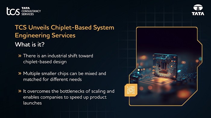
Tata Consultancy Services (TCS) launched its Chiplet-based System Engineering Services on September 11, 2025, marking a significant step in accelerating semiconductor innovation in India. This initiative is designed to help semiconductor companies develop faster, more efficient, and powerful chips by harnessing chiplets—small integrated circuit building blocks—at a time when global demand for advanced semiconductors is rapidly increasing. The launch supports India's ambition to become a major global semiconductor hub amid the booming domestic market and government backing through the India Semiconductor Mission.
Key Highlights of the Launch and Its Industry Relevance
-
The service enables semiconductor companies to push beyond traditional chip design constraints, offering flexibility, scalability, and faster time to market.
-
India’s semiconductor market is currently valued at $45–50 billion (2024-25) and expected to more than double to $100–110 billion by 2030.
-
The ₹76,000 crore India Semiconductor Mission (ISM) supports local chip design, fabrication, and manufacturing capabilities.
-
India is home to 20% of the world’s chip design engineers, with global players investing heavily in the country's semiconductor ecosystem.
-
TCS’s new services provide access to world-class chip-to-system engineering expertise, enhancing the competitiveness of Indian and international chipmakers.
Understanding Chiplets and Their Industry Impact
Chiplets represent a paradigm shift in semiconductor design, moving away from traditional monolithic chips where transistor scaling is hitting physical limitations. Instead, chiplets are modular, smaller integrated circuits that can be combined to form complex multi-chip systems. This modularity allows:
Faster product launches by simplifying design complexity.
-
Reduced development costs and risks through reusable components.
-
Superior performance via tailored combinations suited to specific use cases.
-
Enhanced signal integrity, lower latency, and compact multi-chip packaging using advanced technologies such as 2.5D and 3D interposers and multi-layer organic substrates.
TCS’s Role and Capabilities in Chiplet Engineering
-
TCS brings over two decades of semiconductor industry experience and extensive investments in next-generation technologies. Its chiplet engineering services cover:
-
Comprehensive design and verification for key industry standards like Universal Chiplet Interconnect Express (UCIe) and High Bandwidth Memory (HBM).
-
Advanced packaging design solutions focusing on multi-chip modules that optimize performance and manufacturability.
-
Collaborative projects, such as one with a leading North American semiconductor firm, which modernized chip design approaches by integrating heterogeneous chips, accelerating AI processor deployment.
Supporting India's Semiconductor Ecosystem Growth
The launch aligns perfectly with the broader government initiative, the India Semiconductor Mission, aiming to transform India into a semiconductor manufacturing and design powerhouse. TCS’s technology expertise and global footprint:
Strengthen India’s semiconductor R&D capacity.
Propel innovation by democratizing access to cutting-edge chip design methodologies.
Reinforce partnerships with global semiconductor firms seeking to leverage India as a strategic design and engineering hub.
Market Response and Industry Outlook
As the semiconductor industry faces unprecedented demand driven by AI, cloud computing, electric vehicles, and IoT devices, chiplet-based system engineering is poised to become a critical differentiator. TCS’s newly launched services put India on a competitive edge globally, helping chipmakers accelerate tape-out cycles and deliver scalable, high-performance chip solutions.
Shares of TCS showed optimistic movement post-announcement, reflecting market confidence in its semiconductor innovation strategy.
Source: Tata Consultancy Services Press Release, Business Standard, Economic Times, The Hindu Business Line, and Fortune India .
Advertisement
Advertisement