


Loading market data...
ADVERTISEMENT

Latest Top News
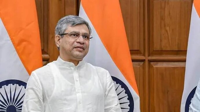
India Greenlights ₹4,594 Crore Investment for Four Semiconductor Projects Across Three States
In a major push to strengthen India’s semiconductor manufacturing ecosystem, the Union Cabinet has approved four new semiconductor projects with a combined investment of ₹4,594 crore. The announcement, made by Information and Technology Minister Ashwini Vaishnaw on August 12, 2025, marks a...
Stay Ahead – Explore Now! Vijay Deverakonda, Rashmika Mandanna Award Scholarships to 180 Students
ADVERTISEMENT

Latest Updates

From Silt to Sustainability: BMC Starts Rejuvenati...
15 Jun 2026, 02:01 PM
Jharkhand Secures GI Tags for Bhagaiya Silk and Tr...
15 Jun 2026, 02:24 PM
Reel Deal: Mumbai International Film Festival 2026...
15 Jun 2026, 10:07 PM
Nepal Tea Trade: Factories Shut Down Over India’s...
15 Jun 2026, 10:03 PM
Motorola’s Foldable Fold-Off: Which New Razr Fits...
15 Jun 2026, 09:59 PMADVERTISEMENT

Top Stories
From Silt to Sustainability: BMC Starts Rejuvenati...
15 Jun 2026, 02:01 PM
Jharkhand Secures GI Tags for Bhagaiya Silk and Tr...
15 Jun 2026, 02:24 PM
Reel Deal: Mumbai International Film Festival 2026...
15 Jun 2026, 10:07 PM