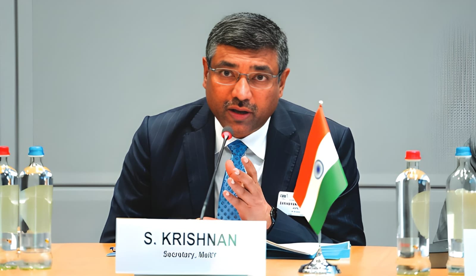

India’s Ministry of Electronics and Information Technology (MeitY) has announced plans to aggregate order demand from domestic fabless semiconductor firms. Led by Secretary S. Krishnan, this strategic policy leverages pooled volumes to negotiate better manufacturing rates, lower minimum order sizes, and priority access from global foundries.
NEW DELHI — The Indian government is moving to aggregate order volumes from domestic fabless chip design companies to help them negotiate better pricing, lower minimum order quantities, and secure priority production slots with major global semiconductor foundries.
Speaking on August 23, 2026, S. Krishnan, Secretary of the Ministry of Electronics and Information Technology (MeitY), outlined the strategic initiative aimed at strengthening India's position in the global semiconductor value chain. While India accounts for nearly 20% of the world's semiconductor design talent, local startups and smaller design firms frequently face commercial disadvantages when dealing individually with overseas commercial foundries. By pooling order demand, the government aims to leverage collective volume to grant domestic companies leverage comparable to multinational tech conglomerates.
Government Mechanism to Support Local Fabless Ecosystem
Under the proposed demand aggregation model, MeitY will act as a facilitating body to consolidate chip design requirements from domestic firms before presenting aggregated order books to international foundries. Small and medium-sized chip designers often struggle with high tape-out costs and strict minimum wafer-start requirements imposed by global foundries. Aggregating demand allows multiple Indian firms to participate in multi-project wafer (MPW) runs and bulk production contracts, significantly reducing capital barriers.
"The strength of India's domestic semiconductor industry lies heavily in chip design," stated S. Krishnan, Secretary at MeitY. "By aggregating demand from multiple design houses, we can secure significantly better commercial terms, priority access, and reduced costs from global foundries for Indian companies".
The initiative aligns with the expanded India Semiconductor Mission (ISM 2.0), which broadens state support across design, manufacturing, advanced packaging, and research and development.
Economic Impact and Industry Context
India's domestic demand for semiconductors is projected to reach $200 billion. As local electronics manufacturing expands rapidly across automotive, consumer electronics, and telecom sectors, establishing a competitive fabless design sector is critical to reducing import dependency.
For domestic startups, lower foundry costs accelerate time-to-market and reduce burn rates, enabling more viable commercial deployment of locally designed microprocessors, power management ICs, and AI hardware components. For international foundries, the initiative provides a structured, predictable pipeline of aggregated orders from India’s fast-growing hardware ecosystem.
Official Sources Section
According to official releases from the Ministry of Electronics and Information Technology (MeitY) and statements made by MeitY Secretary S. Krishnan, the government is finalizing structural guidelines for the demand aggregation policy. Official statements confirm that the policy forms a cornerstone of the broader India Semiconductor Mission (ISM) framework to foster self-reliance in high-tech manufacturing.
Quote Section
"According to ministry officials, aggregating order volumes resolves a longstanding operational bottleneck for Indian startups, allowing domestic chip designers to compete on cost parity with global firms when negotiating wafer allocation with international semiconductor foundries".
Why It Matters
For Tech Startups: Lowers capital barriers to commercialize chip designs by reducing individual tape-out and wafer manufacturing costs.
For Domestic Electronics Manufacturers: Ensures a stable, cost-effective supply of locally designed semiconductors tailored to regional hardware needs.
For Investors: Reduces operational risks and capital requirements for venture-backed fabless semiconductor companies operating in India.
Key Facts at a Glance
Lead Agency: Ministry of Electronics and Information Technology (MeitY).
Core Objective: Aggregate demand from Indian fabless chipmakers to negotiate superior pricing and production terms with global foundries.
Market Outlook: India's semiconductor consumption is targeted to double to $200 billion.
Strategic Alignment: Operating under the broader India Semiconductor Mission (ISM) incentives.
Frequently Asked Questions (FAQ)
What is fabless chip design?
Fabless chip design refers to companies that focus exclusively on designing and developing semiconductor microchips while outsourcing the actual physical manufacturing (fabrication) to specialized third-party foundries.
How does demand aggregation help small semiconductor companies?
Small design firms often lack the scale to meet high minimum order requirements or command favorable pricing from commercial foundries. Aggregating orders combines multiple smaller contracts into a single large request, securing volume discounts and priority manufacturing schedules.
Does India have domestic semiconductor foundries?
India is currently constructing several semiconductor assembly, testing, and fabrication units under the India Semiconductor Mission (ISM), with initial projects slated for commercial production. In the interim, Indian fabless firms rely on global foundries for advanced node fabrication.
Source: Ministry of Electronics and Information Technology (MeitY) | India Semiconductor Mission