Prime Minister Narendra Modi has inaugurated India's third semiconductor plant, a ₹7,600 crore CG Semi OSAT facility in Sanand, Gujarat. Marking the realization of a 60-year national vision, the plant initiates commercial production of automotive and 5G chips, establishing Sanand as a major global silicon packaging hub.
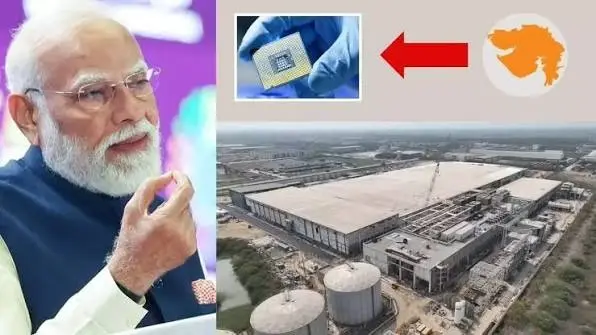
SANAND — Prime Minister Narendra Modi officially inaugurated India’s third domestic semiconductor manufacturing facility on Saturday, July 4, 2026, marking an unprecedented milestone in the country’s high-tech industrial journey. Located in the Sanand GIDC industrial estate in the Ahmedabad district of Gujarat, the state-of-the-art Outsourced Semiconductor Assembly and Test (OSAT) plant has been established by CG Semi Private Limited with a total capital investment of ₹7,600 crore. The commercial commissioning of the facility marks a crucial phase under the ₹76,000 crore India Semiconductor Mission (ISM), shifting the country from an intellectual design provider to an active commercial producer in the global silicon value chain.
A Historic Breakthrough for Domestic Chip Packaging
The launching of commercial chip manufacturing at the Sanand site officially resolves a long-standing structural deficit in India's electronic ecosystem. The high-tech plant is managed via a joint venture anchoring CG Power and Industrial Solutions with Japan’s Renesas Electronics Corporation and Thailand’s Stars Microelectronics.
The technical architecture of the facility is engineered to process both mature, high-demand legacy chips and next-generation packaging form factors. Operating with a projected dual-facility roadmap, the complex is scaling up to achieve a combined daily output capacity of 1.5 crore semiconductor units. The initial production runs are targeted explicitly at supplying critical chips to automated components in the automotive sector, high-velocity 5G telecommunication hardware, industrial equipment arrays, and heavy power applications.
The packaging capabilities deployed inside the cleanrooms include:
Quad Flat Packages (QFP): Standard surface-mount legacy processors for automotive microcontrollers.
Quad Flat No-Leads (QFN): Low-profile silicon footprints optimized for high-efficiency power switches.
Flip-Chip Ball Grid Arrays (FC-BGA): High-density advanced packaging configurations built for 5G network transceivers.
Unprecedented Execution Speeds Outpace Global Models
Speaking on the sidelines of the launch event, Union Minister for Electronics and Information Technology Ashwini Vaishnaw highlighted the extraordinary pace of the domestic rollout. While Western technology subsidies under the US CHIPS Act have faced multi-year corporate gridlocks over labor rules and environmental assessments, India's pari-passu (equal-footing) central co-investment model has cleared industrial pipelines at record speeds.
The rapid sequencing of Gujarat’s semiconductor hub illustrates this operational velocity:
Micron Technology ATMP: India's first packaging unit, commissioned in Sanand in February 2026.
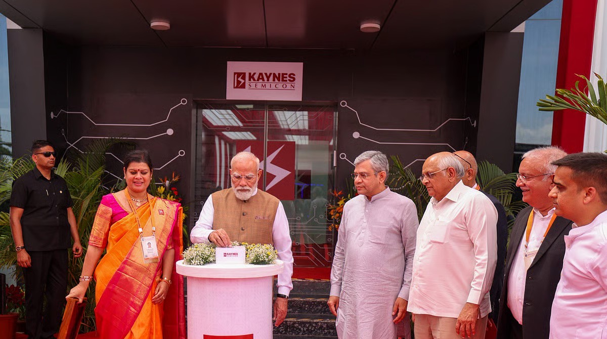
Kaynes Semicon OSAT: The second high-capacity facility, operationalized in Sanand in March 2026.
CG Semi OSAT: The third operational plant, launched commercially today.
Vaishnaw noted that under the guidance of Prime Minister Modi, the CG Semi plant transitioned from its initial cabinet approval in February 2024 to an active, verified commercial production unit in less than 28 months. The Minister stated that by the end of 2026, four independent semiconductor plants will be fully functional across India, with Tata Electronics' $11 billion mega-fabrication plant in Dholera targeting its first commercial wafer output by December 2026.
Transforming Sanand into India's Chip Cluster
The rapid concentration of capital transforms the regional economy from a traditional automobile manufacturing center into India's first high-scale chip packaging cluster, mimicking Hsinchu in Taiwan and Gyeonggi in South Korea. Under the regional support frameworks of the Gujarat Semiconductor Policy, the state has systematically deployed ready-built industrial utilities, specialized high-voltage grid stability nodes, and direct water pipelines to prevent volatile production breaks.
From an employment standpoint, the newly commissioned facility currently maintains a workforce of 300 highly specialized silicon engineers. The structural expansion of the site over the coming five years is projected to generate upwards of 5,000 direct and indirect specialized jobs. To feed this high-tech talent pipeline, the state has integrated curriculum updates across 315 universities, ensuring that regional engineering graduates possess certified mastery over global chip design tools.
Official Sources Section
The engineering parameters, financial outlays, project histories, and investment details cited across this comprehensive report are verified through official joint communiqués issued by the Ministry of Electronics and Information Technology (MeitY), Government of India, state infrastructure dossiers published by the Chief Minister's Office (CMO), Government of Gujarat, and corporate regulatory filings submitted by CG Power and Industrial Solutions Limited.
Quote Section
The strategic validation of the semiconductor ecosystem was underscored heavily by central and state leaders during the inauguration ceremonies.
Reflecting on the historical significance of the chip launch, Union IT Minister Ashwini Vaishnaw stated:
"Today is a historic day. Today, India's third semiconductor plant will be inaugurated by PM Narendra Modi in Sanand. The semiconductor industry has been a national priority for the last 60 years. Finally, it was possible with the vision and execution of Prime Minister Narendra Modi. A lot of hope for the country has been fulfilled for many years."
Addressing the public gathering at the Sanand compound, Prime Minister Narendra Modi stated:
"Our goal is not limited to establishing a single factory, but to building an entire ecosystem. India is now focusing on the complete semiconductor value chain, which includes all levels from design engineers to machine manufacturers and logistics. The rapid growth of India's semiconductor sector will make this decade the biggest turning point in the country's technological future."
Why It Matters
The commercial operationalization of CG Semi’s plant holds vital practical implications for local auto corporations, electronic manufacturers, and global supply chain security. By manufacturing legacy and advanced chips within national boundaries, India minimizes its exposure to sudden geopolitical bottlenecks and oceanic freight shocks that have historically crippled production lines. For international technology corporations, the state’s rapid project execution speeds and substantial fiscal support offer a reliable, alternative hardware production base, accelerating global supply chain diversification away from historically concentrated hubs.
Key Facts at a Glance
The Milestone: Prime Minister Narendra Modi has officially inaugurated India's third semiconductor plant in Sanand, initiating international commercial chip shipments.
The Investment: The advanced OSAT facility represents a specialized capital layout of ₹7,600 crore, executed via a global joint venture.
Production Volume: The facility operates legacy QFN/QFP lines alongside advanced FC-BGA modules, targeting an ultimate joint capacity of 1.5 crore chips per day.
Employment Creation: The project is modeled to generate 5,000 highly specialized direct and indirect technology jobs over the next five years.
National Vision: IT Minister Ashwini Vaishnaw confirmed the launch successfully realizes a 60-year national policy goal to localize silicon packaging.
FAQ Section
Q: What exactly is an OSAT facility, and how does it differ from a fabrication plant?
A: OSAT stands for Outsourced Semiconductor Assembly and Test. While a fabrication plant (fab) prints raw circuits onto silicon wafers, an OSAT facility takes those completed wafers, cuts them into individual dies, packages them inside protective, conductive housings, and tests them for final market deployment.
Q: Which corporate entities comprise the CG Semi private joint venture?
A: The ₹7,600 crore facility is co-funded and operated as a joint alliance between India's CG Power and Industrial Solutions, Japan's Renesas Electronics Corporation, and Thailand's Stars Microelectronics.
Q: Where are the other two operational semiconductor facilities located in India?
A: All three of India's initial operational packaging plants are located within the Sanand industrial cluster in Gujarat: Micron Technology's ATMP unit, Kaynes Semicon's OSAT plant, and the newly launched CG Semi facility.
Source: Policy indices and project updates from the Ministry of Electronics and Information Technology (MeitY), press bulletins from the Press Information Bureau (PIB) India, and operational statements from the India Semiconductor Mission (ISM) Portal.